10 convincing reasons why engineers should consider electroforming
Nov 29, 2016 7:00:00 AM By Maarten NijlandAs an engineer, you want to get your innovations to the market as fast and as cheaply as possible. This short time-to-market requires short lead times, high operational efficiency and cost-effective and large-scale production. On top of that, components are becoming smaller and smaller — while high-precision requirements stay intact. To properly deal with these requirements, utilizing the right technology is crucial. In this blog, we mention 10 reasons why electroforming is a suitable manufacturing method to deal with your engineering challenges.
1) Significant cost reduction
With an additive manufacturing technique like electroforming, metal objects are built up atom by atom. As a consequence, you use almost every piece of metal, resulting in virtually zero waste of material. The reduction of waste is a very direct way to enable cost reduction through additive manufacturing.
In other manufacturing processes such as milling, the production costs increase along with the complexity of the part. This isn’t the case with electroforming.
2) Large scale production and high replicability
With a method like laser processing, every metal part needs to be individually cut out. When we look at milling, the machine needs to mill every piece one by one, which directly affects the time that is required to produce larger volumes. Electroforming allows you to simultaneously grow a large number of high-tolerance parts onto one mold.
The more metal pieces that are needed, the more interesting electroforming gets. Electroforming is perfectly suitable for small and large series because the complexity of the part has limited or no effect on the manufacturing time. High replicability is a great benefit that comes with electroforming.
3) High-precision metal parts
A lot of industries see an increasing demand for metal parts of very high precision. To meet this demands, parts need to be created at micron or even submicron level — something conventional techniques such as laser cutting or stamping simply can’t do.
Electroforming is the technique to create high-precision metal parts. You can utilize electroforming to make products where the standard deviation of its most critical feature is only ~0.1 µm on that single part!


4) No additional tooling (costs)
With some techniques, you’ll need additional tooling before you can start the creation process. Take die-cutting, for example, which requires a punch to produce output.
When you use electroforming, the production of your metal parts depend on the creation of a perfect mold. A mold is created by applying a geometric pattern to a sensitive resist on a substrate by means of light. This was — and still is by many companies — typically done by placing a mask on a photoresist layer and exposing light to the entire mask. But with the arrival of the Laser Direct Imager, the mask has become redundant. The Laser Direct Imager (LDI) is capable of projecting high-resolution images directly from a CAD file! This process makes electroforming a cost-effective technique because you do not require additional tools.
5) Freedom of design
The creation of components straight from your CAD file is an obvious indicator of freedom in your design process. And because you can grow a large number of parts onto one mold, electroforming also provides engineers with a lot flexibility.
Electroforming is very suitable for what is called the experimental approach: a design method where you create up to a couple of dozen versions of your component (depending on the size of your component) to see which one works best for your product. If you want varying samples of your component — instead of immediately working on your final design — electroforming may be the solution for you.
6) Short lead and delivery times
In stamping, for example, a die may take up to months to build. In CNC Punching, a die is available within days to weeks. After that the realisation of the die, the creation process is yet to be initiated. A mold that is used for electroforming, on the contrary, can be produced within hours by utilizing the Laser Direct Imager. Electroformed samples can, therefore, be created and delivered within 3 weeks — and usually even sooner (depending on the complexity of the component).
7) Creation of multi-layer metal parts
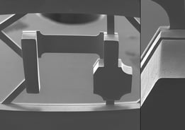
 With electroforming, you are not limited to 2D structures because you can grow additional layers in different directions. As an engineer, you have the possibility to design multi-layer metal parts for your components. These additional layers typically reinforce thinner electroformed parts, making them easier to handle and less fragile. Multi-layer can be best described as 2,5D, as it approximates the feel of 3D. If your goal is to add more structure to high precision metal parts, multi-layer electroforming is highly suitable.
8) Creation of components with very specific contour shapes
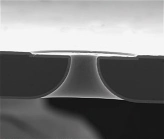
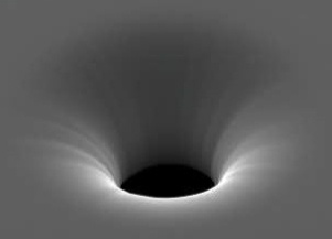
Electroforming allows you to manufacture components with very specific contour shapes — so specific that they cannot be reproduced by other techniques. An example is the overgrowth that is created in an inkjet nozzle plate; the most critical component of an inkjet printhead.
We can go even smaller when we look at nozzle plates that are used in nebulisers. These nozzle plates release millions of micron-sized droplets per second through its unique geometry, forming a perfect fine mist for targeted delivery to the lung.
9) Straight and burr-free side walls
Some components require extremely straight and burr-free side walls. This accuracy is hard to achieve with other techniques. With laser processing, for example, you will often end up with side walls that are rough on the edges. With electroforming, your side walls will be burr-free and extremely straight.
10) Local variation in material properties
Engineers require components with varying material properties. One engineer may require a surface that is as reflective as a mirror, while another engineer may want a product that absorbs as much light as possible. Similarly, one engineer may require a product that is as stiff and hard as possible, while another engineer requires a much softer product with a low elastic modulus. An engineer might even require a component that has both light-reflecting and light-absorbing properties.
All of these material properties alterations can be achieved by manipulating the crystal structure of your material — something you can do effectively with electroforming.
Your engineering challenges and electroforming
There are a lot of benefits that come with electroforming, and some of them particularly solve the challenges you have as an engineer. Short lead times, high operational efficiency, continuous innovation, cost-effective and large-scale production — you can accomplish these goals by utilizing the right manufacturing method. Electroforming may just be the technique that will help you become a better engineer.
If you’d like to learn more about electroforming — and want to find out if it’s the technique that fits your engineering needs — you should check out our electroforming whitepaper:


