Electroforming is recognized as a high-precision manufacturing technique for two-dimensional metallic components. This process, however, may not suffice for certain intricate metal components that necessitate exceptional accuracy and comprehensive three-dimensional structuring. In such cases, multi-layer Electroforming emerges as the preferred method.
What is Electroforming?
Electroforming is a highly precise metal fabrication process that forms metal parts through electro-deposition. It is acknowledged to be one of the best technologies in the precision metal fabrication industry today. Its uniqueness is that you can grow metal parts atom by atom. The technology allows high replicability while staying highly accurate.
Multi-Layer Electroforming
Multi-layer Electroforming is an advanced manufacturing process that builds upon the core principles of standard Electroforming. The main reason to add more layers in other directions to a metal part - and therefore create the 3rd dimension - is that multi-layer metal parts provide a more delicate structure. Also, they can also improve strength to reinforce very thin parts, making them easier to handle and less sensitive to potential damage.
To add multiple layers to the metal parts, the same Electroforming process is repeated. With multi-layer Electroforming, 3D or 2.5D structures can be achieved, which opens up the window for demanding high-precision components that also demand delicate structures. Below are two applications that benefit from multi-layer structures.
Applications of Multi-layer Electroforming
The multiple layers bring new possibilities for many industries that demand precision metal solutions. Below are examples of how multi-layer Electroforming enables breakthroughs in the Digital Printing and Solar Energy industry.
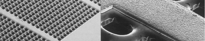
Inkjet Nozzle Plates
Inkjet nozzle plate is a good example of a multi-layer Electroformed metal part. The image below shows an inkjet nozzle plate and ink chamber. In this case, the nozzle plate was electroformed using the overgrowth method (plating defined), and subsequently, the ink chamber was electroformed using the thick resist method (photo defined).


Solar Cell Stencils
Solar cell stencil used for solar cell printing is another good example. Precision stencils are taking the place of conventional wire meshes or emulsion screens with increasing demand for energy efficiency in the industry, and electroformed solar cell stencils in particular proved to be the best choice for solar cell printing.
Hard nickel stencils can be electroformed in both single layer and double layer.
Is multi-layer electroforming the right solution for your application?
If your goal is to add more structure to high-precision metal parts, multi-layer electroforming might just be the perfect solution for you. Electroforming is the solution to raise the bar on precision, tolerance, cost-effectiveness, and the capability to withstand high temperatures.
As application of Electroforming is only limited by imagination, the engineers of Veco always like to be challenged to design and create your next innovation. Feel free to talk to one of our engineers about your new challenge!