The electroforming process explained: highly customized metal precision
Jul 18, 2017 8:00:00 AM By Harrie KnolAs you may already know, products made through electroforming can be implemented in versatile ways and in a wide range of industries. The precision metal solutions created through electroforming not only put many companies in more competitive positions in the market, but also enable innovative breakthroughs. But how does the process work?
And, more importantly, how exactly does this particular process provide advantages for your end product that other precision metal processes simply can't? In this blog, the electroforming process is explained thoroughly enough for you to pick out the key essentials.
Building metal on micro scale accuracy
Electroforming is known as a highly accurate additive manufacturing process. It's important to know that it is also an electrodeposition process. Electrodeposition is the deposition of metal onto a conductive object. How is this done? Two electrodes (a +ve anode and a -ve cathode) are placed inside an electrolytic bath, containing a solution of metallic salts and a power source of direct current (DC). While the anode dissolves the material, the cathode builds up - forms - the material. In other words, metallic ions are converted into atoms which build up onto the cathode surface through a continuous deposit. Therefore, the material can be built up on micro scale accuracy: you could even say atom by atom!
Control the thickness and shape of the end product
Depending on the material used and the size of the substrate, thanks to the electric charge in combination with the time span, the electroforming process makes it possible to control ampere seconds, minutes or even hours (and therefore the thickness of the formed material) extremely accurate. This makes it possible to create the product in a desired thickness at micron accuracy.
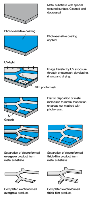
Thickness of the plated part brings a new challenge to the table. To control shape of the product, metal is grown onto a patterned surface: the substrate. Two different methods with different outcomes can be applied: electroforming overgrowth and electroforming thick resist. Read more in our free electroforming whitepaper.
 Plating defined: electroforming overgrowth
A light sensitive coating is applied on a conductive surface. Artwork, film or glass-tooling, is used to expose the light sensitive coating. The coating will polymerise where it is exposed to UV light.
After developing the light sensitive coating the mandrel with conductive and nonconductive areas is ready for electroforming. Metal will grow over the photo resist and size of the apertures is defined by the overgrowth of the electroforming process. Accuracy of the product is therefore defined by the plating process.
Photo defined: electroforming thick resist
In some cases, it is desired to make the product thicker. This is when the thick resist method is applied. The mandrel surface is masked off with photoresist except for the hole area in the pattern. You don't grow over, but build the metal between the shape, resulting in a pattern with a cylindrical hole shape. Thus in this case accuracy is defined by the photolithographic process.
No matter how the electroforming process is applied, in the end it will result in perfect process control, high quality production (accurate hole size, burr and stress free holes and sharp edges). This makes electroforming perfectly suitable for low cost production, high volumes and high repeatability.
So, how will electroforming enable your next innovation? Discover it by downloading our free electroforming whitepaper.
Inside you'll find:
- The process in practice: how a customized inkjet nozzle plate is made
- Industry solutions: breakthroughs enabled by electroforming
- Electroforming vs etching: which one to choose?

