Electroforming is a versatile Additive Manufacturing process for the production of high-precision and complex metal parts. This article provides an overview of key features and capabilities that make Electroforming a crucial manufacturing technology for engineers to get acquainted with.
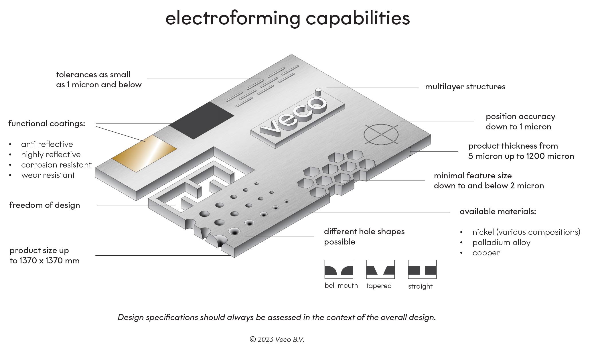
tolerances below 1µm
Electroforming enables extremely high precision and accuracy in producing fine details and complex geometries. It can fabricate parts with tolerances as tight as below 1 micron. This degree of precision is enabled by combining advanced lithography with highly controlled Electrochemical deposition and accurate replication. The tight tolerances offered by Electroforming make it a critical technology in industries where even the smallest deviation can significantly impact the performance of the end product.
various functional coatings available to meet different demands
Coatings can enhance the properties of the Electroformed components, making them more suited to specific applications. At Veco, a variety of functional coatings are provided, such as anti-reflective coatings for superior optical performance, reducing glare, and enhancing the clarity of the transmitted image. In contrast to anti-reflective coatings, highly reflective coatings are used to maximize the reflection of light. They find applications in various fields, including solar energy, lighting, and optics. Moreover, With wear-resistant coatings, component lifespan can be effectively extended, while corrosion-resistant coatings can protect components against harsh environments.
freedom of design
Electroforming unlocks unprecedented freedom of design for intricate metal components. The Electroforming process empowers engineers to explore creative, complex geometries without being constrained by conventional manufacturing limitations. It facilitates rapid prototyping of engineer designs with sophisticated shapes and intricate details typically seen as not manufacturable with conventional manufacturing processes (check comparison of Electroforming and other precision metal manufacturing processes here ). The extraordinary design flexibility is further leveraged by Electroforming’s capability to produce highly complex parts without excessive tooling costs or lead times.
multi-layer structure
Electroforming has evolved beyond its origins as a process for simple two-dimensional metal sheets and foils. Advanced multi-layer Electroforming now enables the fabrication of complex three-dimensional structures through a layer-by-layer buildup method. This layer-by-layer fabrication approach facilitates the creation of complex geometries and internal structures impossible to produce using conventional subtractive methods.
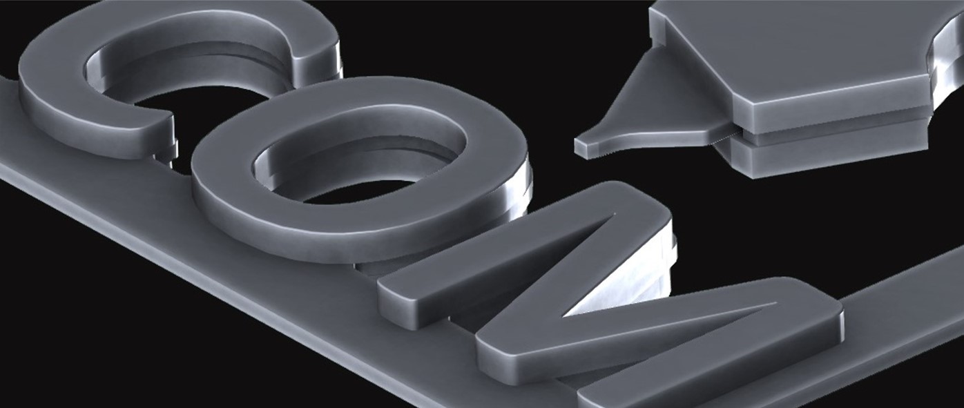
different feature cross-sections
Electroforming allows precise fabrication of metal parts with diverse cross-sectional shapes, straight-walls, tapered profiles, and bell-mouth shapes that can be produced through advanced process control. Veco utilizes two distinct Electroforming processes - Plating defined and Photo defined. The plating defined method creates bell-mouth-shaped cross-sections by modulating current density during plating. The photo-defined technique uses patterned resist layers of varying thickness to form straight-walled geometries. These two methods can be combined to provide engineers with a high degree of design flexibility to meet specific functional needs.
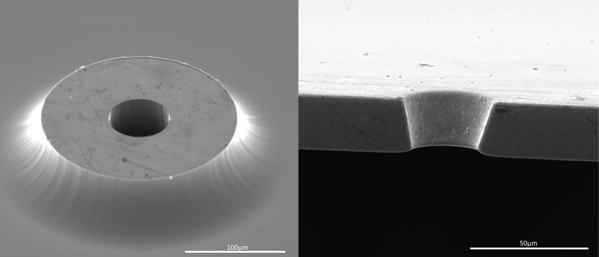
position accuracy down to 1 µm
The position accuracy achievable with Electroforming reaches the micron level. This micro-scale accuracy empowers the fabrication of components with intricate details positioned exactly as designed, making it an ideal choice for applications where precision is paramount, such as in the fields of optics, aerospace, medical devices, and microelectronics.
available materials
As the industry-leading Electroforming specialist, Veco expands material capabilities, offering not just commonly used Nickel and Copper, but also a variety of proprietary alloys tailored for specific applications. These include Meta-Nickel for thermal resilience and mechanical robustness, Sulfamate Nickel for high ductility and low internal stresses, Palladium-Nickel for bio-compatibility in combination with superior resistance, HR-Nickel for thermal stability, and Veco84 - Veco’s specially formulated nickel with superior hardness and strength.
feature size down to 2 µm
Electroforming is capable of producing metal components with microscopic feature sizes down to 2 microns. With this micro-scale resolution, Electroforming facilitates the production of miniaturized components with delicate details for applications from micro-electronics to micro-optics. Tiny holes, channels, pillars, and other geometries can be incorporated to meet mechanical, fluidic, or optical requirements.
product size up to 1370*1370mm
Electroforming provides a scalable solution for large yet intricate metal parts. Through advanced equipment and process control, Electroformed parts can be fabricated with dimensions up to 1370 x 1370 mm. The combination of part size and precision empowers innovation in new domains that demand both high accuracy and macro-scale dimensions.
product thickness from 5µm to 1200 µm
Electroforming enables precise control over a broad deposit thickness range spanning from micrometers to millimeters - thin layers down to 5 microns and thicker deposits up to 1200 microns. This broad thickness range allows Electroforming to meet the needs of diverse applications from delicate MEMS structures to robust macro-scale components.