Additive manufacturing (AM) is a manufacturing method that uses the deposition of materials to build up components layer by layer. You can see additive manufacturing as a ‘from-the-bottom-up-method’. Additive manufacturing is also referred as additive layer manufacturing, layer manufacturing, additive fabrication, etc.
Common additive manufacturing methods are:
- Electroforming
- 3D printing
- Material jetting
- Binder jetting
- Material extrusion
- Directed Energy Deposition (DED)
Additive manufacturing is the opposite to subtractive manufacturing, a manufacturing method that entails the removal of materials to produce a component. You can look at subtractive manufacturing as a ‘from the top down method’. Common subtractive manufacturing methods are:
- Chemical etching (also known as photo etching, chemical milling, industrial etching, etc.)
- Laser cutting
- CNC machining
- (micro) Punching
Additive manufacturing vs. subtractive manufacturing: when to choose what?
There is such a wide variety of both additive and subtractive manufacturing methods that we zoom in on two specific techniques to create a tangible comparison: electroforming, an additive manufacturing method; chemical etching, a subtractive manufacturing method. We address some important engineering factors in this comparison.
Precision
Needless to say, size is important. And when we say micro, we mean micron! Both technologies meet tight tolerances. What are we looking at when we express the standard deviation of the material thickness in percentages?
In electroforming, experts claim to deviate less than 1 μm (= 0,001 mm) of the materials thickness. The rule of thumb most people stick to is +/- 5% of the thickness of the material. Tolerances quoted on etched features will typically be +/- 10%. So when a part of 200 μm is chemically etched, the deviation might be 20 μm (0,02 mm).
Shape/hole geometry
In some industries, shape or hole geometry plays a significant role when considering different technologies.
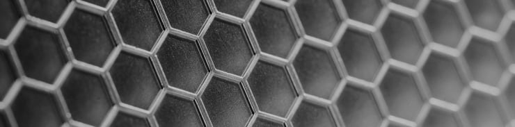
In electroforming, two methods can be applied to control thickness and shape: electroforming overgrowth and electroforming thick resist. The unique shape resulting from the overgrowth method proves it's a method one can simply not realize with other techniques. Electroforming, therefore, lends itself to complex features and special shapes.
The chemical etching process doesn't allow for control of the hole shape like electroforming does.
Material (and hardness)
Choice of material is also an important factor when selecting the right manufacturing method.
In electroforming, nickel is predominantly used, followed by palladium nickel or copper. On the other hand, virtually all metals can be chemically etched with no restriction in hardness of the material.
However (!), properties of nickel — in particular, hardness — can be controlled in electroforming. Nickel has a controlled hardness of 200 to 670 HV (Vickers). You may not want to pinpoint on a material (such as stainless steel) but rather on the flexibility in properties of the material. This might open new doors in truly picking the right technology to create your metal parts.
Chemical etching might be a more suitable solution when your material is predetermined, and nickel is not the choice.
Cost-effectiveness
There is one aspect we haven't discussed yet in the choice between chemical etching and electroforming: which technology is the most attractive-looking from a price perspective.
A rule of thumb is: the higher the precision, the higher the price. But a rule of thumb always comes with exceptions. Manufacturing costs of electroformed products are, in many cases, less than the manufacturing costs of chemically etched products. However, compared to e.g. stainless steel, nickel is relatively expensive and has a significant influence on the price of the final products. When nickel is your preferred material, electroforming is generally the preferred technology to make your products, both from a precision and commercial point of view.
If you would like to learn more about the possibilities of additive manufacturing — and electroforming in particular — we advise you to check out our electroforming whitepaper: