Electroforming is an Additive Manufacturing technique based on the electrodeposition process, with the unique advantages of high dimensional precision and replication accuracy. As miniaturization continues to be a driving force across various industries, Advanced Lithographic Electroforming is gaining significant attention for its ability to fabricate micro-precision components. It excels at achieving strict dimensional tolerances and intricate geometries, making it a crucial solution in the ever-evolving landscape of manufacturing. The scalability of Advanced Lithographic Electroforming sets it apart from traditional Electroforming processes. Due to its non-contact nature, it can efficiently handle high production volumes while maintaining consistent quality and precision across numerous micro-precision components. This article dives into Advanced Lithographic Electroforming, as well as micro-scale LIGA Electroforming technologies such as UV LIGA and X-Ray LIGA.
Electroforming technology
Electroforming is a metal fabrication process that works on the principle of electrodeposition, similar to Electroplating. It can be used to produce metal parts by electrochemically depositing metal onto a mold, as well as to replicate metal parts with high precision. Common metals for the Electroforming process include nickel, gold, copper, etc.
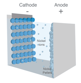 The electrodeposition process starts with a conductive mandrel which is placed in an electrolytic bath and the electrodes pass a DC through the solution. The DC current converts ions into a metallic deposit on the conductive areas of the mandrel until the desired thickness has been achieved. Compared to other traditional metal forming technologies, for example, casting, forging, stamping, or deep drawing, Electroforming can deliver mass volume at superior accuracy and extreme design complexity, due to the fact that it can replicate the shape of the mandrel at extreme accuracy.
Advanced Lithographic Electroforming
Veco, as the world leader and largest independent supplier of Electroforming, has been moving the industry forward, with unparalleled experience in Electroforming, advanced lithography technology, and accumulated knowledge of metallurgy. Veco’s unique Advanced Lithographic Electroforming is also referred to as Advanced Photo Electroforming.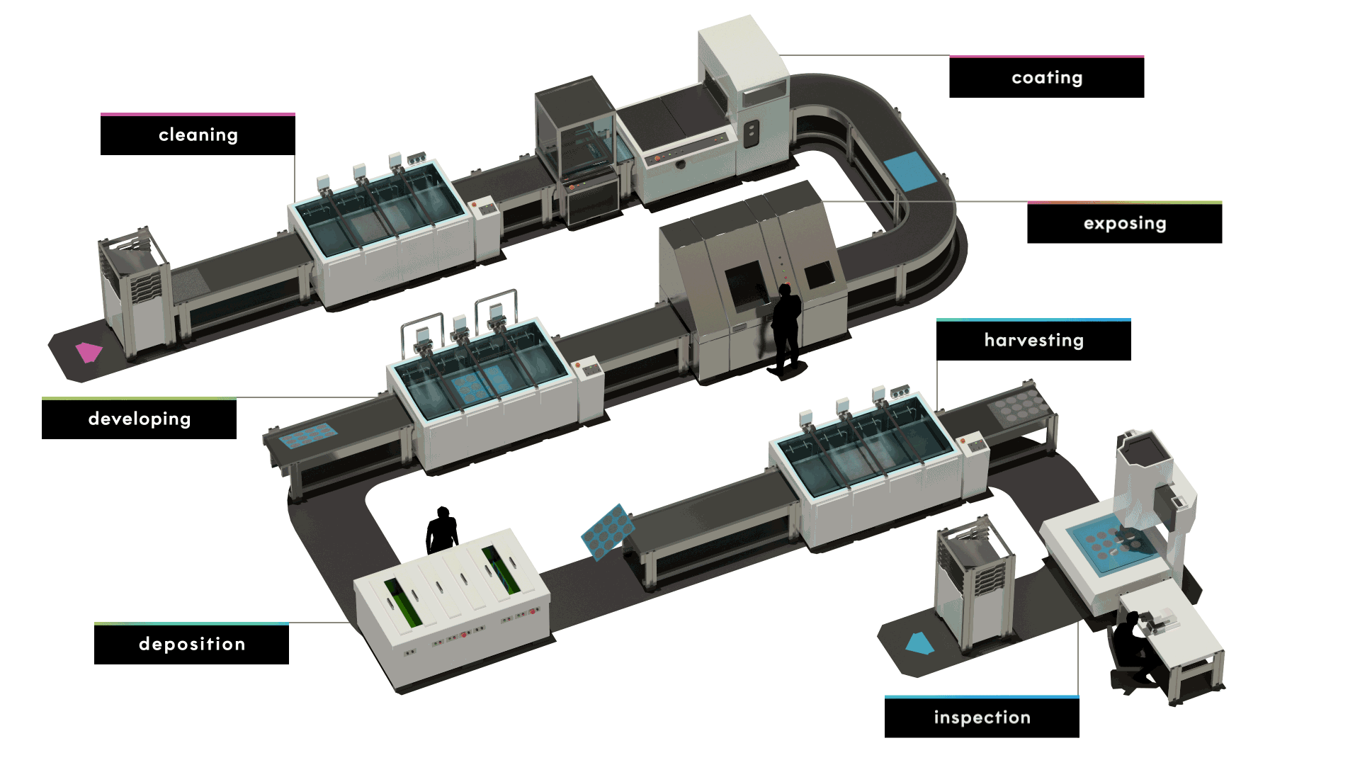 At Veco, LDI(laser direct imager) is used to expose the photoresist layer directly on the substrate. It allows for rapid prototyping and design changes, as the laser patterns can be easily adjusted and updated without the need to create new physical masks or tools. This flexibility enables faster and more cost-effective iterations in the design process, compared to the time-consuming and expensive process of fabricating new glass tools for each design change.
At Veco nowadays, 90% to 95% of our photolithography process is done by Laser Direct Imaging. The combination of LDI and our leading Electroforming technology has enabled us to further push the boundaries of the industry with our Advanced Lithographic Electroforming, providing our customers with high-precision metal components of higher quality, at lower cost, and with a quicker turnaround.
LIGA Electroforming: UV LIGA, and X-Ray LIGA
LIGA is a German acronym for "Lithographie, Galvanoformung, Abformung", which translates to "Lithography, Electroplating, and Molding". In LIGA Electroforming, a photoresist such as SU-8 or PMMA is patterned using photolithography to create a mandrel for electrodeposition.
UV LIGA is a LIGA process that uses UV light to expose photoresist through a photo mask. With UV LIGA, a thicker layer of photoresist can be penetrated, enabling a higher aspect ratio, which is an advantage in many applications. X-Ray LIGA is another variation of the LIGA process that uses X-ray radiation instead of UV light to expose the photoresist. The process involves placing a substrate coated with a thick layer of photoresist in an X-ray synchrotron beam, which exposes the photoresist in the desired pattern. With X-ray, even thicker layers of photoresist can be penetrated, allowing for extremely high aspect ratios exceeding 100:1, which is not achievable with UV LIGA or LDI processes.
Comparison of LDI-empowered Lithographic Electroforming and LIGA Electroforming technologies
When comparing LDI-empowered Advanced Lithographic Electroforming and LIGA Electroforming technologies such as UV LIGA and X-Ray LIGA, many factors come into play. Here we compare on level of precision, cost efficiency, and scalability:
Precision: LDI-empowered Advanced Lithographic Electroforming has a high resolution comparable to UV LIGA and X-Ray LIGA, enabling the fabrication of high-precision microstructures.
Cost Efficiency: The production cost of LDI-empowered Advanced Lithographic Electroforming is significantly lower compared to UV LIGA and X-Ray LIGA due to the avoidance of expensive photomasks and long exposure times.
Scalability: LDI-empowered Advanced Lithographic Electroforming is the most scalable while X-Ray LIGA has very limited production volume, and UV LIGA can be used for mass production but limited volume. Moreover, it has high repeatability and lower costs compared to LIGA Electroforming technologies.
In summary, Advanced Lithographic Electroforming offers the necessary high precision and geometry complexity for micro precision metal parts, combined with fast prototyping, high volume suitability, and cost efficiency, making it the ideal process across the product lifecycle from prototypes to mass production.
Table. Technical specifications of Advanced Lithographic Electroforming and LIGA Electroforming
|
Technical Specification |
LDI |
UV LIGA |
X-Ray LIGA |
|
Exposure |
UV laser |
UV light |
X-ray |
|
Resolution |
High |
High |
Very high (due to shorter X-ray wavelength) |
|
Aspect ratio |
Limited (due to thin layers of photoresist and limited depth penetration depth) |
High (due to thick layers of photoresist and good depth penetration depth) |
Extremely high ,exceeding 100:1 (due to excellent depth penetration depth) |
|
Prototype Speed |
Fast (as no photomask is needed) |
Moderate (photomask required) |
Slow ( photomask and synchrotron beam time required) |
|
Scalability |
Highly suitable |
Suitable, but limited volume |
Very limited |
|
Cost efficiency |
Significant cost advantage |
Moderate |
Very expensive |
Interested to learn more about Advanced lithographic Electroforming? Don't miss out on our Electroforming Whitepaper.