During the annual Precision Fair, the annual meeting point for precision technology in The Netherlands, Harrie Knol gave a speech about micro manufacturing techniques and surface treatment. More specifically, advantages of Electroforming in the world of micro manufacturing.
Transcript below:
Harrie Knol: Thank you for the introduction. You were quite positive I will try to make it an interesting presentation. I will do my utmost to achieve that. Yeah again, welcome. I’d hoped for a somewhat bigger audience, but as I already said to my introducer, it might also have to do with our technology. We are 80 years in the electroforming business, but it’s still quite an unknown technology. Together with photo-etching, electroforming is quite an unknown technology. So, I will try to change that this afternoon.
I’ve made a short agenda: so, the intention of this presentation, then the introduction to the electroforming process, electroforming in the world of Micro Manufacturing, and then advanced some examples of electroformed products, something about automation and especially based on the inspection we’re doing, and then at the end there should be some time for questions or even discussions.
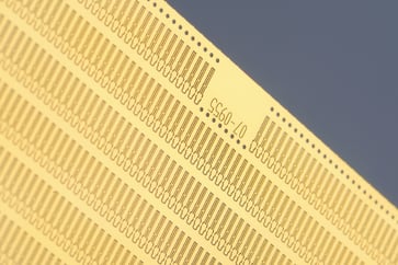
My intention of this presentation: explain that electroforming is an additive manufacturing process, growing atom by atom. And we all know additive manufacturing is very popular at this moment due to 3D printing, I’ll come back on that later. And then I will want to enthuse, not especially young men, but engineers for the electroforming technology. As I already explained, it’s still a quite unknown technology. And make you aware that electroforming is able to make high-volume production with micron tolerances. Here you can already see an example. There’s an example of a shaver foil.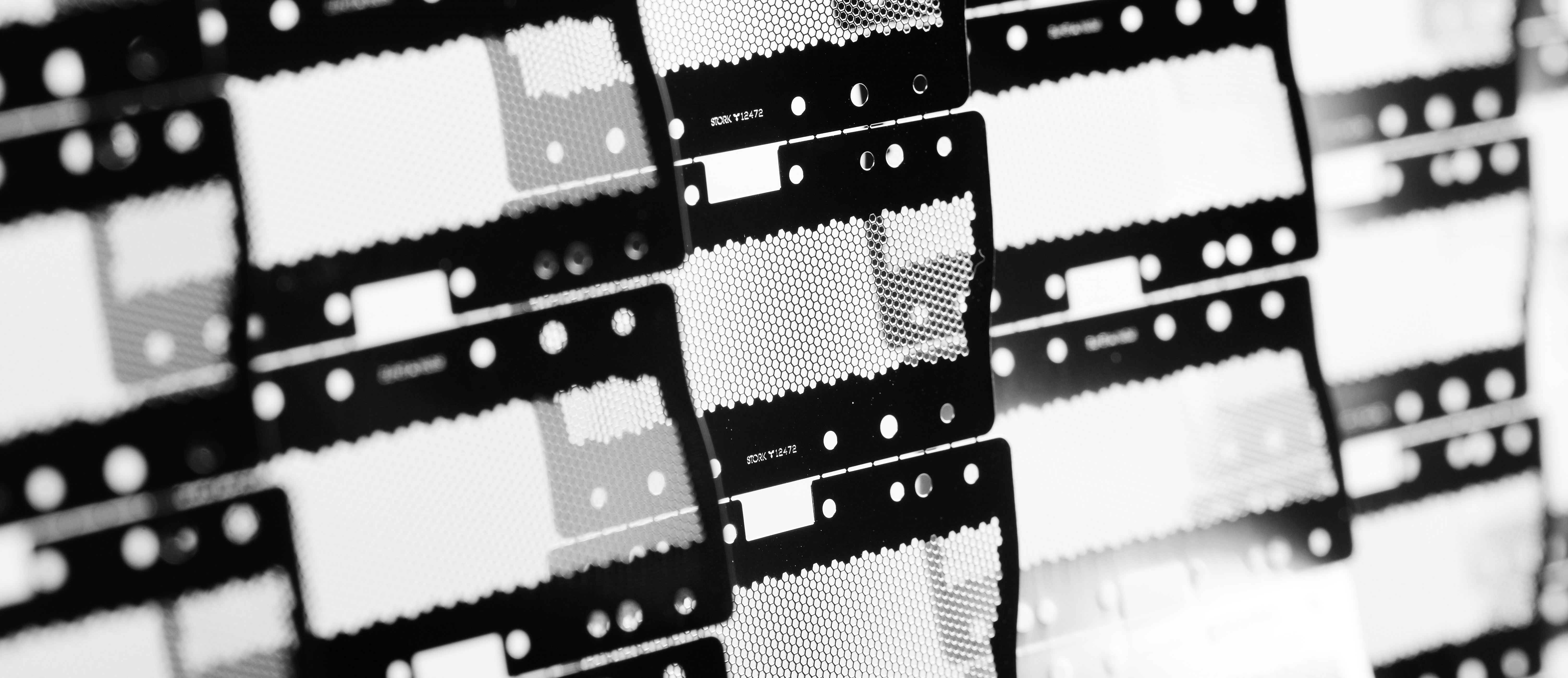 Shaver foils are made annually 100 million pieces per year. At Veco in the Netherlands, we produce 30 million of them and we do it with only two persons. What I mean to say is that it’s quite a mature technology. You can really make high-volume with micron tolerances. This one is not that critical, we make them on square meter mandrels, typical tolerances here are plus/minus five, plus/minus ten. But again, you can make them in very easy and very high volumes. And also show you some nice animations and with the invitation if you like them, to do your next development together with us, with Veco.
The process itself. It’s, as I said, additive manufacturing, building your materials atom by atom. So, in fact, we don’t make holes, we make the materials around the holes. Of course, we sell holes, but we make the material around the holes. We start with a metal substrate, metal or glass, it depends on what kind of product and what our requirements are. It has to be conductive so if it’s glass you have to coat it with metal or whatever – or not whatever. You have to coat it with a metal, sorry.
Then we apply a coating, a light sensitive coating. It can be a dry-resist, it can be a very thin, positive resist. I will get back on that later. Then we expose the photoresist and you’ll get a mandrel with conductive and non – this is the non-conductive and this is the conductive area. Then you can deposit nickel, copper, or some kind of alloy, what you want, and then you can electroform the pattern. And this animation already shows two types of patterns. We can go over the resist and we can go between the resist, but I’ll come back on that later. And after stripping the photoresist, we can easily harvest the product. And in fact, we have nearly, totally freedom of design. You can make anything.
So, this is how it looks in practice. I won’t read all the text again, but again, additive manufacturing, atom by atom. So, we have nickel pallets in the solution, that’s the anode. You apply a current and then the nickel will deposit in the cathode, electroforming any product or any shape you want.
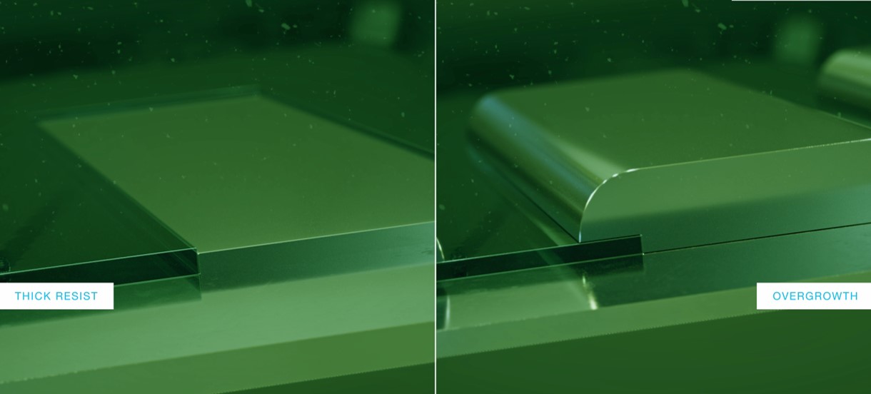
As I already said with the previous slide, we have two types of electroform. We have what we call plating defined. What you see here is this yellow line, that’s the photoresist. When we start electroforming, the nickel builds up, builds over the photoresist and here you can see that it’s a completely isotropic process. So, the thickness is exactly the same distance as this one. So, with this process, we have to be very accurate on the thickness. Why? For example, here you see an inkjet nozzle plate. In this inkjet, we have to make them, we have to produce ‘em in high volumes in plus/minus one micron. That means the thickness is coming from both sides, so the thickness has to be within one-half, within a half micron accuracy, over a substrate of 30-30 or even up to square meter, but this one typically is made on substrates that are 30 by 30.
Because the hole size depends on the thickness of the metal deposits, we call it plating defined. So, the plating bath affects, at the end, the hole size that you can make, that you can grow.
This is what we call photo defined. Here we have a very thick photoresist, and in fact what we do if we grow the nickel, also between the photoresist, these are the typical hole shapes you’re making with these thick resists. And this is called photo defined or lithographic defined because you’ll become independent from your plating solution. It doesn’t matter if you make a micron less or more. It doesn’t matter the hole size, they’ll be exactly the same and that’s why we call it photo defined.
Surface replication is also possible, so not a thick or thin material, but the previous speaker, Max Groenendijk, he was talking about making all kind of surfaces. Recently we have some projects with him, so if you can make a structure micro-nano structure with his laser, with his pico- and femtosecond laser, we can very easily transfer it into the positive or the negative, build a family of it, scale it up, and even the smallest details up to square meter size can be replicated rather easily and used as a mold for the industry or organization.
There are few steps I want to go through, this one very fast because I also have an animation. We have to prepare the substrate, can be metal, can be glass. We apply a photoresist, in this case it’s a laminate, it’s a dry photoresist, but we can also apply a wet resist. Then we do the photo imaging. In the past it was done with mylar artwork if it’s fairly accurate. For example, if it’s inkjet production we use glass tooling, but more and more we’ve switched to a laser direct imaging, meaning that you can directly write into your photoresist. After that, the resist is developed.
Putting it in electroforming but in here you can see the typically overgrowth, the plating defined, and this is the photo defined, so this is done with thick resist. And after stripping the photo resist, we can easily peel off the product sand make thousands or millions of products, whatever we want.
Video Animation 1 (Harrie’s Narration): So, this is the animation of the whole process. So that’s also substrate fabrication, then we can apply photoresist, dry resist. Pre-exposure with a laser direct imaging. And the photoresist is developed. Substrate is taken to the forming bath. Again, there are two types of electroforming, you can do overgrowth. And the photoresist is removed and if you do it in a correct way, the products won’t stick to your mandrel, you can easily pull them off in half a stroke. It depends on how accurate we have to be. Let’s say plus/minus one, we do one 30 by 30, plus/minus three 50 by 60 centimeters, and plus/minus five, plus/minus ten, we have mandrels up to one and a half by one and a half meter. This enables us to make millions and millions of products. For example, an encoder disc with slits of 30 microns, nebulizer for drug simulation 2-micron holes, 60-micron thickness, an inkjet nozzle plate with holes of 15 micron.
Harrie: And again, you have totally freedom of design. I think we have more than 1400 active customers annually.
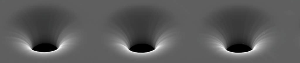
Again, additive manufacturing. High aspect ratio, for example, the nebulizer you saw for the drug simulation has a 2-micron hole, 60-micron thickness. That’s what we mean with aspect ratio. You can’t achieve that with etching, you can do it with laser, but I’ll come back on that later, it’s too slow. Accurate hole size, not only accurate, but also if he promises a 10-micron hole, you get a 10-micron hole. So also, for filtration that’s very important, if he promises you a 10-micron hole, you should have a 10-micron hole to do an absolute filtration and not to do an in-depth filtration, where you can use let’s say, 2 to 20 microns. But if we say 10 microns, it will be 10 microns. Micron sized holes, non-clogging holes, I will also get back on that later.
Yeah, we have three core technologies: electroforming, photoetching, and laser cutting. Today, I want to focus on electroforming. The advantage of electroforming, yeah, you can make huge quantities of products with both technologies but with the electroforming technology, you can very easily achieve tolerances up to ten times better than with photoetching. Sometimes the material parts can be adjusted to the customer needs. For example, the nebulizers, they have to be bio compatible and we work with palladium nickel, these type of things. Same story for laser cutting. Laser cutting is evolving very fast, especially the pico- and the femtosecond laser, and specifically in the area we are in the micron area. But it’s still far too slow and with electroforming it doesn’t matter. If you make one hole or you make a thousand or even a million holes, you all do it in the same time. But I have to be honest, I said material parts can be adjusted to the customer needs, but I have to be honest, with photoetching and with laser cutting you have more freedom to choose your material. With electroforming it’s mainly nickel or copper and it’s alloys.
Electroforming is as I said additive manufacturing, very popular due to 3D printing. Here you can see a General Electric fuel nozzle. It’s also made by additive manufacturing. They were quite successful with this part and in 2020 they are about to produce 45 thousand of these fuel nozzles. What we do is also additive manufacturing, but it’s not as 3D as this one is, but we can also make very nice products. I thought we could –
Video Animation 2 (Voiceover): Introducing machines of incredible complexity, designed to exacting precision, and created without assembly. Machines of unparalleled performance and unprecedented scale. Welcome to the genesis of micro machines. This extraordinary process begins with a 3D CAT model using proprietary software. The model is divided into layers allowing photomasks to be generated to submicron accuracy, with hundreds to even thousands of devices fitting on a single ceramic wafer. A custom photography process defines a pattern where the first layer of structural metal is deposited at the atomic level through electro deposition. The photoresist is then dissolved, and sacrificial metal is deposited over the structural material. The surface is then planarized to a consistent uniform thickness within a tolerance of two microns. The process is repeated for each layer in the design defining a new standard for the creation of complex mechanisms. The sacrificial metal is then abstracted through a chemical etching process, simultaneously enabling movement of each mechanism while releasing the device from the wafer. High performance micro machines and precision parts, enabling new solutions in medical, semiconductors, and aerospace.
Harrie: I did put this animation in. I have to be honest with you, it’s not something we do at Veco, at Eerbeek, but I wanted to show you the atomic or the additive manufacturing layer by layer. As we all know it’s done by layers, you can also do it with electroforming. There are companies involved in it, if you’re interested, please contact me and I will get you in contact with these people. But I only want to show you in the previous movie that you can do it also the layer by layer manufacturing and make moving parts also by electroforming.
Some product examples we are currently producing. This is a mold for making hooks in composite materials. Some materials these pillars they are made for cleaning purposes. We can -- This is only a hundred micron, but we can make it on square meter. This is in fact currently the smallest product we are making. It has a diameter of 15 micron, the slit is about six to seven microns, so you can imagine if you a substrate 30 by 30 you have millions and millions of products. But on the other hand, we make very small products. This is done in a clean room, let’s say class hundred, but we can also make products on one and a half by one and a half meters. Here is a typical example, it’s a screen to filter the sugar crystals out of the molasses and I think in Eerbeek we produce about two on the square meter of these.
All kind of other applications. I want to start with this one. It’s a measurement equipment to measure sensors in autonomous driving cars. And to the sensors here on the tips, we can put all kind of features on top of it. And these features they should make contact with the solder ball on the tips to enable, to measure the chips into an autonomous driving car. And here you can also see all kinds of tips, and this is a typical one. And it presses into the solder ball so you’re able to measure the function of a part.
Some other examples, inkjet is a very industrial ink jet also used for 3D printing, especially the industrial one is an important market for us. Nozzle diameters 15 to 60, it’s more of 15 to 40. More and more they get to 15 microns and tolerance is plus/minus one, but if you go to 15-micron hole size, plus/minus one is not enough anymore. We make them in very big quantities. And why do people like these electroform plates? As you can see here, the hole is very symmetrical, and this is a cross section of an electroformed hole. Here you can also see that we have in this case applied a gold plating. It’s more and more changed into palladium nickel because it’s cheaper and it’s easier to apply, but in this one there was a gold plating. But what the inkjet customers, what they like is that the hole is very symmetrical, and you get a superior jet straightness. The big ones, let’s say the Ricohs, Seikos, the Konica Minoltas, Xerox, Canon, Fuji, they are all working with electroform nozzle plates or they want to go back to the electroform nozzle plates just because of the superior jet straightness. There’s also another discussion to which it’s -- the metal is quite rigid, and they can get into higher frequencies due to the rigidness of this nickel product.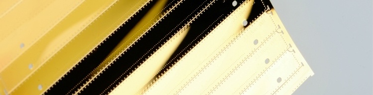
The nebulizer plates, I’ve mentioned them quite often already, hole sizes is down to two microns, 60 microns thick, biocompatible, in this case we made them in palladium nickel. We do not only make them for the drug simulation, also for perfumes, pesticides, humidifiers, whatever, but this one is for the medical industry.
Video Animation 3 (Voice Over): Our unique palladium vibrating mesh technology is a breakthrough in aerosol drug delivery and is at the heart of all our products. And unlike traditional small volume nebulizers, both the Aerogen Solo and the Aerogen ultra are virtually silent in use. The central aperture plate is just 5 millimeters in diameter and perforated with one thousand precision formed holes. This vibrates 128 thousand times per second creating a mini pump that produces a fine particle mist of uniform sized droplets, each between one and five microns in diameter, an ideal particle size for dep lung penetration. Clinical studies have shown that this results in deposition rates far greater than can be achieved by conventional nebulization. Both the Aerogen Solo and the Aerogen Ultra offer incredible versatility confirming Aerogen’s commitment to a new era high performance aerosol drug delivery throughout the hospital environment.
Harrie: Here it’s very important these holes are about two microns, the droplets it would each release four to six microns and that means that the drug directly disappears into your body. If they are too big, if they are bigger than eight to ten microns, they will congregate in your lungs and then the positive effect of the nebulizer is gone, because the positive effect is that you need, let’s say, five to ten percent of the drugs you would normally need when you take it oral. And it’s not because of costs or anything, but it’s just because of the side effect of these medicines, if you can use five or ten percent you don’t have all of these negative side effects of these drugs.
Test Contactors, also a fast-growing market. I already mentioned autonomous driving car, there are coming more and more sensors into these cars. They all have to be measured and also these contactors, they are very small. On 30 by 30 centimeters there are about 30 to 40 thousand of these contactors on it. And they are used to make contact between the printed circuit board and the solder ball from the process, which enable us – well not us but our customer to measure these sensors.
Although there are many different designs, high volume production, millions and millions, all different types, this one is milled, but this one is electroformed, this is one we are currently making. And again, we can make all kinds of types of features or whatever we want because we have quite a – there are a freedom of design in our products.
I think, automation and inspection. Of course, we want to automate as much as possible, especially in the larger series, but also in the production you already saw. But I think here we really make the difference with our competitors. If you promise to make an inkjet with an orifice plus/minus one, you must also be able to measure it. We do measure these products, really, 24/7, even over the weekend this machine is running, I will show it later in an animation. Data management is an integral part of supply, that means that all the data are stored and are sent with the products to our customer. So, his product placement team knows exactly where the rejects are, and they will take them out.
And at the end for the nebulizer, we can do punching, doming, function-test, and packaging all in one machine, completely automated, and no one involved.
This is an animation and I think it’s says quite a bit. I was talking about automation and it starts with manual inspection, but please –
Video Animation 4 (Harrie’s Narration): So, this is the robot I was talking about. These sheets are 30 by 30 centimetres, several thousand holes in it, and it will take him a couple of – let’s say with hundred thousand holes in it, it will take half of or three-quarters of an hour for a sheet to have it completely measured and have the data stored. Encoder discs, here we don’t measure, we punch them out and after that we do a function test. We know what signal the customer wants to get from this product and we don’t measure it, but we do a function test. They are completely 100% tested on function. Here you can see the function test and it will decide ‘okay’ or ‘not okay’ and will be shipped to the customer. Surface inspection, this is something we at this moment we do at a small scale. Each individual part has a bar code in it, so we know exactly what is measured and what part is measured and where it comes from, when it has been made. We do it just on small scale, we are learning on it, but within a half year we will be able to do it on sheets from 50 by 60 centimetres so each dust particle or whatever will be removed or rejected automatically. This is a typical inkjet, surface of such an inkjet. And here is the tape and reel machine, I already mentioned. So, the all-size measurement, the doming, the punching, measuring, the dome height, and at the end package them and tape and reel it’s all done completely automatic in one machine.