What is Electroforming? 3 types of Electroforming explained.
Apr 10, 2018 7:00:00 AM By Maarten NijlandElectroforming is an additive manufacturing process specialized for the production of high precision metal parts. Its uniqueness is that you can grow metal parts atom by atom, providing extreme accuracy and high aspect ratios. Electroforming is also an electro-deposition process, which we've illustrated in a previous blog.
In this article we will introduce 3 types of Electroforming: Electroforming Overgrowth, Electroforming Thickresist, and Surface Replication with Electroforming.
(1) Plating Defined Electroforming: the Overgrowth Method
Plating defined electroforming is also referred to as an overgrowth method.
Fig 1. Schematical cross section of an overgrowth product (in blue) on a thin photoresist pattern (in orange).
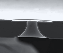
It uses a thin photoresist pattern to shield parts of the conductive substrate. A light-sensitive coating is applied to the conductive surface, and it will polymerize where it is exposed to UV light. Metal grows over the photoresist and the thickness of the product (T) exceeds the thickness of the photoresist (TR), hence the process is also known as overgrowth.

The process is mainly used to make sheets with small conical orifice s for filtra tion and (ink)jetting.
Note that outer corners will round off during growth,while inner corners will be sharp.
Fig 2. cross section of an overgrowth product.
(2) Photo Defined Electroforming: the Thick Resist Method
Photo defined electroforming is also called the thick resist method.
Fig 3. Schematical cross section of a product (in blue) deposited between a thick photoresist pattern (in orange).
In some cases, it is desired to make the product thicker. This is when the thick resist method is applied. A thick pattern of photoresist is used during photo defined growth, such that the thickness of the product (T) does not exceed the thickness of the photoresist (TR).
Aspect ratios (TR/ WR) up to 1 can generally be achieved with ease. The exact limits depend on the size and geometry of the products .
(3) Surface Replication with Electroforming
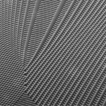
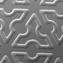
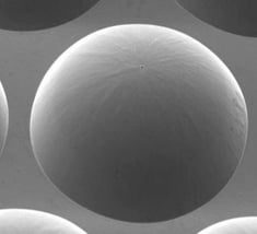
The electroforming process allows for extremely precise duplication of the mandrel. The high resolution of the conductive patterned substrate allows finer geometries, tighter tolerances, and superior edge definition. This results in perfect process control, high-quality production and very high repeatability.
Electroforming is therefore perfectly suitable for high precision surface replication at low cost and in high volumes.


Fig 4-6. Examples of surface replication by electroforming
To learn more about Electroforming, such as what are the major types of Electroforming, technical capabilities of Electroforming, key benefits of Electroforming, as well as applications of Electroforming, download our free whitepaper of Electroforming, or feel free to talk to one of our Electroforming engineers!

