The trend in many industries is towards smaller, more complex and more delicate devices with higher levels of performance. Miniaturization is no longer a wish; it is a necessity we see across all kind of industries.
There are many advantages that come with the creation of increasingly smaller products, but it’s good to also be aware of the corresponding challenges — because designing smaller parts doesn’t mean you can lower product performance expectations.
Quite the opposite is true: basic materials — like metals — used to transform designs into actual products must perform better than ever before, since the smallest irregularity will have a much larger effect on the end result. In this blog, we discuss test contactors to illustrate this dynamic.
High-performance test contactors for semiconductor testing
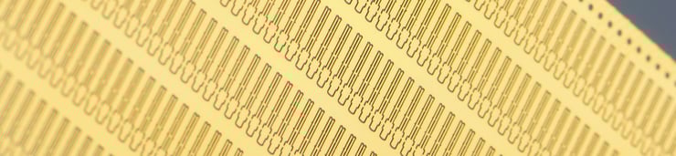
Test contactors are used to determine the performance of electrical devices like micro-electro-mechanical systems (MEMS), sensors, microcontrollers and integrated circuits. The probes are used in the semiconductor and automotive markets for pre-launch validation and production tests, for instance. With required dimensions as small as a few micrometers, engineers in the semiconductor industry need micro-precision manufacturing solutions that provide great reliability as well.
Electroforming: the future-proof solution for miniaturized contacts
Electroforming is a method to produce metal parts by precise deposition of metals onto patterned substrates. Its uniqueness lies in the fact that you can grow delicate metal parts atom by atom, providing absolute accuracy and high aspect ratios. Electroforming is an additive manufacturing process specialized for producing ultra-high precision parts. While nickel is typically used as the main component, extensive variants with inter-layers and coatings of various materials are possible, yielding probes that perform optimally.
Let’s take a look at 4 benefits of electroforming in relation to test contactors:
1. Higher precision sub-micron tolerated versatile tubes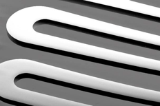
The electroforming process is very flexible: your design can be changed easily without the need for expensive tooling costs. By its ability to produce very fine curved shapes it surpasses conventional technologies like stamping and punching. Radii as small as 30 microns can be made in relatively thick (30-100 micron) material.
2. Higher density and further miniaturization of intercircuits
With electroforming, it is possible to keep up with the demands for HD intercircuits. It is possible to make very slim designs with high aspect ratios. This means that very small products can be made without compromising on reliability. Aspect ratios achieved with electroforming are up to 3 times higher than with conventional stamping or punching.
3. Smoother surface for enhanced reliability
The contact surface is free from burrs, fractures, or stress, which leads to enhanced reliability of the contact products. Also, a combination of materials — as well as surface finishing — is possible to increase the functionality of the product.
4. Better material developed dedicated for increased contact
Special Electroformed materials have been developed to maximize the functionality of the products. Materials up to 600 Vickers hardness with a very high thermal and electrical conductivity exist. The “spring” behavior of these materials results in a very long lasting product without wear.
Electroforming: the future-proof solution for your miniaturization challenges
Once you’ve discovered the benefits of electroforming, a whole new world of opportunities opens up. What if you could produce — atom by atom — stress- and burr-free precision metal parts with micron scale accuracy? What if you could achieve this fascinating result at even lower costs, with shorter lead times? What if you could try out your new design with fast and flexible prototyping and proceed with industrial scale production in no time?
Discover these electroforming benefits — and others — by reading our Electroforming whitepaper.