Electroforming is an additive manufacturing process that forms high-precision metal parts through precise Electrodeposition. It uses a current to deposit metal, usually nickel, onto a conductive mandrel or mold. The mandrel is then removed, leaving a free-standing metal part or shell in the desired shape. While this basic principle remains the same, major improvements have taken place. Veco, the market leader with the largest production facility, has been moving the industry forward with unparalleled experience in Electroforming, advanced lithography technology, and accumulated knowledge of metallurgy.
Veco’s unique Advanced Lithographic Electroforming process also referred to as Advanced Photo Electroforming, promises a move towards the frontier of precision engineering, incorporating micro precision, complex features, and freedom of design, all of which empower next-gen innovations across industries facing the challenge of miniaturization. This blog introduces 5 reasons to choose Electroforming in terms of freedom of design.
(1) A complex design can be easily achieved with Electroforming, efficiently and cost-effectively.One of the biggest challenges engineers face is managing the costs associated with designing and producing complex parts. As part complexity increases, manufacturing expenses tend to rise exponentially due to extra tooling costs, additional set-up and changeover times, and longer processing time, among others. This makes complex designs economically unfeasible for many applications - forcing engineers to limit themselves to "manufacturable" designs.
With Electroforming, complex shapes with intricate details and fine features that are difficult to achieve using traditional metal manufacturing techniques can be quickly tested and implemented, with tooling costs that do not scale with complexity. Thus, Electroforming decouples part complexity from manufacturing expense. This allows engineers to maximize design freedom without worrying about significantly higher costs for more complex designs.
(2) Electroforming offers precise control over material properties.Material properties matter greatly to engineers, with different applications requiring very specific combinations of properties. Choosing the right material for the job is crucial, but in reality, a material's properties depend far more on its internal structure than its basic composition.
Electroforming is a manufacturing process that allows precise control over a material's microstructure and resulting properties. By adjusting Electroforming conditions like current density, pH, and additives, you can alter properties like conductivity, hardness, and elasticity. Does your application require corrosion resistance or low reflectivity or does it come into contact with the human skin? That’s where coatings come in. A layer of material such as palladium or gold can be coated followed by an Electroforming process. This allows engineers to think in terms of the properties needed for an application, rather than the materials, opening up new possibilities.
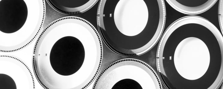 Electroformed optical parts
Engineers often need metal parts with precise cross-sectional shapes to meet certain design requirements or enable specific application functions. This is not easily achievable with other metal manufacturing technologies, which usually provide little control over localized cross-sectional details and shapes beyond constant thickness parts.
Electroforming enables the fabrication of micro-precision metal parts with different cross-sections, both straight-walled profiles and complex tapered-hole shapes can be achieved due to advanced control of the process. At Veco, 2 types of Electroforming processes are available, namely Electroforming Overgrowth and Electroforming Thick Resist. The Overgrowth technique enables the fabrication of tapered cross-sections through variable current density plating, while the Thick Resist method controls the thickness of patterned resist layers to create straight-walled profiles. Finally, these methods can be combined to provide engineers with a high degree of design flexibility considering functional or performance demands for their micro components.
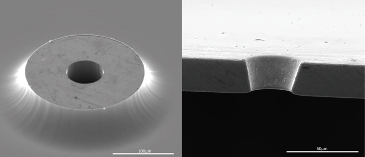 left: straight-walled shape right: tapered-hole profiles
(4) Electroforming is more than 2D.
Electroforming is a metal-forming process that has traditionally been associated with creating two-dimensional metal parts, such as plates, sheets, and foils. This has long been seen as a main disadvantage of Electroforming to many engineers who desire more complex geometries. However, modern advances are enabling electroformed parts to move beyond these 2D limitations.
Multi-layer Electroforming allows building up complex 3D geometries layer by layer - more structures can be added to the high-precision metal parts by Electroforming over a mandrel for one layer, then repeating for successive layers. It is an important technique that expands Electroforming into complex 3D shapes beyond its 2D origins and enables almost limitless part geometries to be produced. The delicate and precise 3D structures it can produce open up new possibilities for more advanced applications.
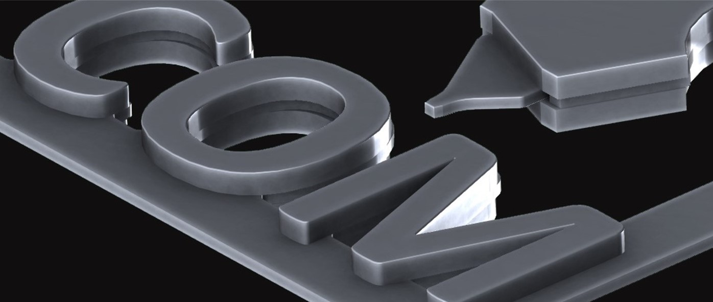
complex part with 3D features
(5) Electroforming is a versatile solution for both fast prototyping and mass production.
Engineers face challenges when seeking a manufacturing solution that can accommodate both fast prototyping and high-volume mass production. Conventional manufacturing methods typically require different tooling and setups which adds time and cost. This places burdens on engineers to compromise on prototypes, over-invest in fixed tools early on, or delay production.
Electroforming is a remarkably versatile process that excels at both rapid prototyping and mass production applications. Even if design changes are required, rapid iterations can be implemented quickly without extra tooling or process changes. This enables tweaks and adjustments at little expense. Electroforming gives engineers the ultimate freedom to bring innovative designs to market with minimal limitations, with the versatility to meet complex demands from fast prototyping to mass production.