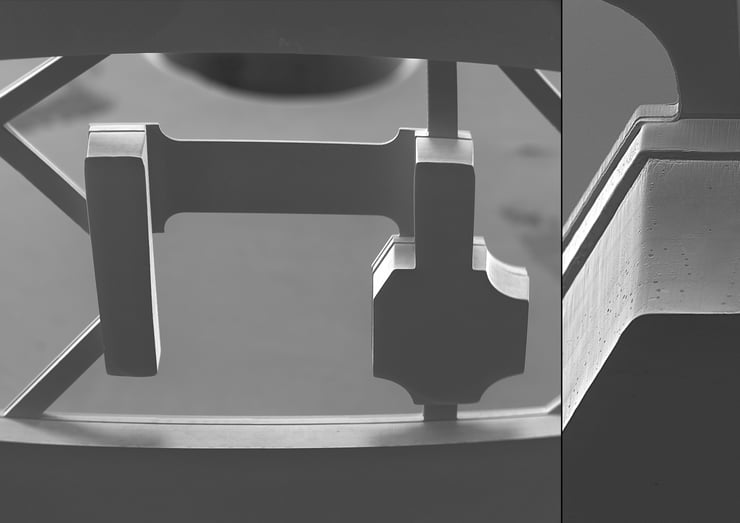
How is electroforming different from other types of additive manufacturing? How does electroforming work?
Jan 20, 2017 9:13:35 AM By Harrie KnolLet’s compare electroforming to the most common and popular additive manufacturing method: 3D printing. Whereas 3D printing applies plastic droplets to build up 3D objects, electroforming builds up precision metal parts atom by atom. Electroforming allows you to “grow” material on micro scale accuracy, providing absolute accuracy and high aspect ratios. Just to give you an idea: experts claim standard deviation of electroformed parts is less than 1% of the material’s thickness.
Because of its high accuracy, electroforming is mainly used for creation of small components and parts rather than entire products. This is how electroforming differs from other additive manufacturing methods like 3D printing.
Most applications made through electroforming are 2 dimensional (2D), unlike products created with 3D printing. However, some industries want their high precision metal parts to provide more structure in all dimensions. This is when multi-layer electroforming comes into play.

The electroforming process explained
It's important to know that electroforming is an electrodeposition process. Electrodeposition is the deposition of metal onto a conductive object. Two electrodes (a +ve anode and a -ve cathode) are placed in an electrolytic bath containing a solution of metallic salts and a power source of direct current (DC). While the anode dissolves the material, the cathode builds up the material. In other words, metallic ions are converted into atoms which build up onto the cathode surface through a continuous deposit. Therefore, the material can be built up on micro scale accuracy: atom by atom.
Two electroforming methods explained
Depending on material used and size of the substrate — and thanks to the electric charge in combination with the time span — the electroforming process makes it possible to control ampere seconds, minutes or even hours (and therefore the thickness of the formed material) extremely accurate. This level of control makes it possible to create the product in a desired thickness at micron accuracy.
Thickness of the plated part brings a new challenge to the table. To control shape of the product, metal is grown onto a patterned surface: the substrate. Two different methods with different outcomes can be applied: electroforming overgrowth and electroforming thick resist.
Plating defined: electroforming overgrowth
A light sensitive coating is applied on a conductive surface. Artwork, film or glass-tooling is used to expose the light sensitive coating. The coating will polymerise where it is exposed to UV light.
After developing the light-sensitive coating the mandrel with conductive and nonconductive areas is ready for electroforming. Metal will grow over the photoresist and size of the apertures is defined by the overgrowth of the electroforming process. The accuracy of the product is therefore defined by the plating process. Check out this video for animated explanation of the overgrowth process.
Photo defined: electroforming thick resist
In some cases, it is desired to make the product thicker. This is when the thick resist method is applied. The mandrel surface is masked off with photoresist except for the hole area in the pattern. You don't grow over, but build the metal within the shape, resulting in a pattern with a cylindrical hole shape. Thus in this case accuracy is defined by the photolithographic process. Check out this video for an animated explanation of the thick resist method.
Industries that benefit from electroforming
Electroforming is very suitable for applications in the following industries:
- Motion control
- Medical devices and systems
- Semiconductor and electronic components
- Optical applications
- Security printing
- Aerospace and aviation
- Automotive
- Laboratory equipment
- Defence
Electroforming has enabled these breakthroughs in industry solutions.
The key benefits of electroforming
Electroforming comes with 10 key benefits. Check out this blog post to discover them all.

